- HOME
-
PCB FAB
For Complex & Reliable Interconnect
For Signal Integrity & Speed
For High Power & Harsh Environments
For Innovative Form Factors
-
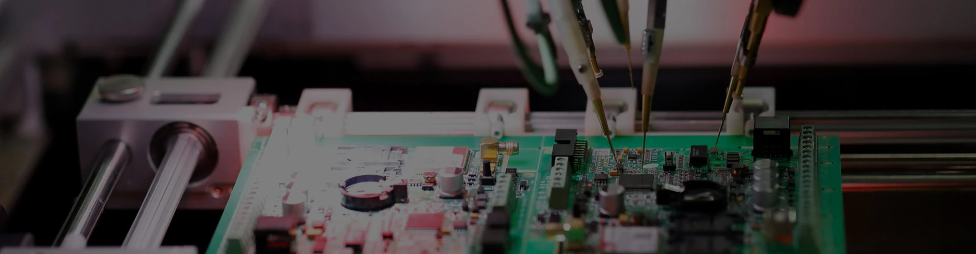
PCBA
PCB Assembly Technologies
PCBA Service Models
Value-Added Services
STENCIL
- CAPABILITY
- ABOUT US
- RESOURCE
- NEWS
- CONTACT
-
-
For Complex & Reliable Interconnect
-
For Signal Integrity & Speed
-
For High Power & Harsh Environments
-
For Innovative Form Factors
-
-
-
PCB Assembly Technologies
-
PCBA Service Models
-
Value-Added Services
-
STENCIL
-
-
-
-
-