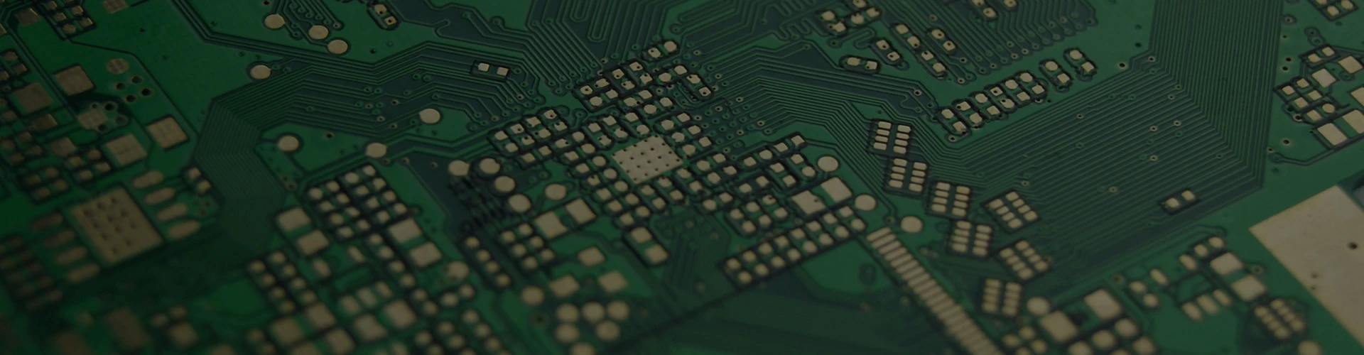
For Complex & Reliable Interconnect
For Signal Integrity & Speed
For High Power & Harsh Environments
For Innovative Form Factors
PCB Assembly Technologies
PCBA Service Models
Value-Added Services
STENCIL
For Complex & Reliable Interconnect
For Signal Integrity & Speed
For High Power & Harsh Environments
For Innovative Form Factors
PCB Assembly Technologies
PCBA Service Models
Value-Added Services
STENCIL
We'd Love to Hear from You
Precision Impedance Control for Reliable High-Speed Performance
Achieving Precise Electrical Characteristics with Advanced Modeling,Tight-Tolerance Manufacturing,and Comprehensive Testing
Guaranteed Signal Integrity:Minimize reflection,crosstalk,and signal distortion.
Expert Engineering Support:From stack-up design to validation testing.
Advanced Modeling&Process Control:Utilizing industry-standard field solvers.
Wide Material Compatibility:From standard FR-4 to high-speed/low-loss laminates.
The Critical Role of Impedance Control in Modern Electronics
In high-speed digital and RF circuits,PCB traces are not simple conductors but transmission lines.When signal edge rates become fast(typically<1 ns)or frequencies rise,the characteristic impedance of these lines must be carefully controlled to match the source and load impedance.Uncontrolled impedance leads to signal reflection,degradation,timing errors,and electromagnetic interference(EMI),causing system instability or failure.
Why Controlled Impedance is Non-Negotiable
Prevents Signal Reflection
Mismatched impedance causes energy to reflect back to the source,corrupting the original signal.
Reduces EMI and Crosstalk
Proper impedance matching contains electromagnetic fields,lowering radiation and interference between adjacent traces.
Ensures Data Integrity
Critical for the accuracy of high-speed data buses(e.g.,DDR,PCIe,USB,Ethernet).
Maximizes Power Transfer
Essential in RF circuits for efficient power delivery from amplifiers to antennas.
Key Parameters & Impedance Models
Controlling impedance requires precise management of several interdependent physical and material properties.
Primary Determining Factors:
● Trace Geometry: Width(W)and Thickness(T)of the copper trace.
● Dielectric Properties: Dielectric Constant(Dk orεr)of the laminate material and pre-preg.
● Stack-up Structure: Height(H)between the trace and its reference plane(s).
● Soldermask: Its coverage and Dk affect the final impedance,typically requiring modeling adjustments.
Common Transmission Line Models:
|
Model |
Typical Use Case |
Key Feature |
Control Focus |
|
Microstrip |
Outer layers (top/bottom) |
Trace on surface, referenced to one plane. |
Trace width, dielectric thickness, copper weight. |
|
Stripline |
Inner layers |
Trace embedded between two reference planes. |
Trace width, core thickness, symmetry. |
|
Edge-Coupled (Differential) |
Differential pairs (USB, HDMI, LVDS) |
Two parallel traces carrying complementary signals. |
Trace width, spacing (S), and consistent coupling. |
SENTAK Impedance Control Tiers:
We tailor our process to your performance needs:
● Standard Control: ±10%tolerance.Suitable for many high-speed digital applications.
● Tight Control: ±7%or±5%tolerance.For demanding interfaces like DDR4/5,Gigabit+Ethernet.
● Advanced Control: ±3%tolerance.For critical RF circuits and ultra-high-speed serial links.
Our Controlled Impedance Workflow:From Design to Validation
A systematic,collaborative approach is essential for repeatable success.
Collaborative Stack-up&Pre-Production Engineering
● Design Submission: Provide target impedance values, net lists, and desired tolerance.
● Impedance Modeling: Our engineers use Polar Instruments SI9000 or similar field solvers with actual material data(Dk, thickness)from our laminate inventory to calculate the optimal trace geometry.
● Stack-up Proposal&DFM Feedback: We return a detailed fabrication drawing with recommended layer stack-up, finished copper weights, and adjusted trace/space rules for impedance layers.We identify any design risks.
Precision Manufacturing with Process Control
● Material Selection&Certification: Use of laminates with stable,certified Dk values.
● Etch Compensation: Advanced CAM software applies precise width corrections based on our etch factor to achieve the final target trace width.
● Layer-to-Layer Registration: Critical for stripline designs.Our equipment ensures precise alignment to maintain consistent dielectric spacing.
● Controlled Lamination: Processes that minimize dielectric thickness variation and resin flow.
Rigorous Validation&Documentation
● Test Coupon Fabrication: Impedance test patterns(as per IPC-2141A)are included in the panel and processed identically to the production boards.
● Time-Domain Reflectometry(TDR)Testing: We use TDR equipment to measure the actual characteristic impedance of coupon traces, verifying conformance to the specified tolerance.
● Comprehensive Report: A Controlled Impedance Test Report, including TDR waveforms and pass/fail status, is provided with your shipment.
Designer Guidelines for Optimal Results
Close collaboration yields the best outcomes.Here’s how to prepare:
Specify Clearly: On your fabrication drawing, list all controlled nets/traces, their target impedance(e.g., 50Ωsingle-ended, 90Ωdifferential), tolerance, and referenced layer.
Prioritize Routing: Route impedance-critical traces first, maintain consistent width, and avoid unnecessary vias or discontinuities.
Define Reference Planes: Ensure a solid, uninterrupted reference plane(GND or power)adjacent to the impedance trace for its entire length.
Include Test Coupons: Allow space in the panel for impedance test structures.We can also assist in designing these.
Engage Early: Involve our engineering team during the stack-up design phase, especially for complex multi-impedance requirements or hybrid material builds.
Applications Requiring Controlled Impedance
This technology is fundamental across advanced electronics sectors:
Data Center & Computing: Server motherboards, SSD controllers, switch/routers (PCIe, SAS/SATA, DDR memory).
Telecommunications: Network infrastructure, optical transceivers, baseband units.
High-Speed Consumer: Gaming consoles, set-top boxes, high-definition displays (HDMI, DisplayPort).
Automotive ADAS: Radar modules, lidar sensors, high-speed camera data links.
Aerospace & Defense: Avionics data buses, radar processing, secure communications.
Your Design Deserves Our Discipline.
Partner with a manufacturer where quality is a measurable, managed outcome.