1.Schematic to Production Pack(Our Recommended&Most Efficient Path)
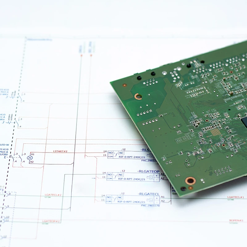
You provide the functional circuit diagram(schematic), and we handle the entire physical implementation.
What You Provide: Complete schematic capture(in OrCAD, Altium, KiCad, etc.), key component specifications, and basic mechanical constraints.
What We Deliver:
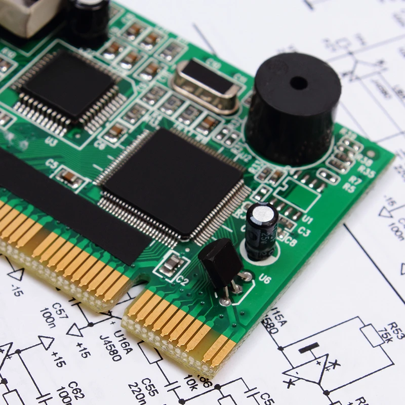
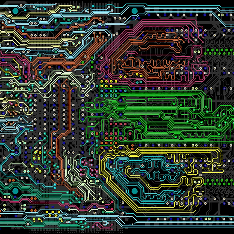
● Manufacturing-Optimized PCB Layout: Layer stack-up design, component placement, routing, power/ground planning, and critical signal handling.
● Industry-Standard Gerber Files: The universal language for PCB fabrication, including drill files and drawings.
● Comprehensive BOM(Bill of Materials): A structured, sourcing-ready list with Manufacturer Part Numbers(MPNs)where possible.
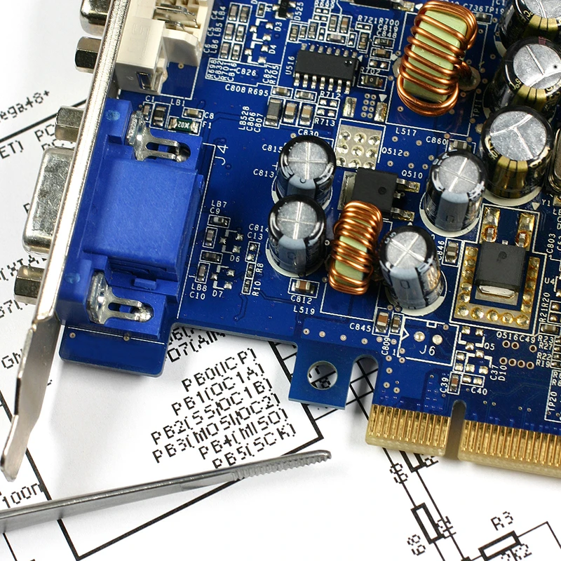
● Assembly Drawings&Pick-and-Place Files: Everything needed for error-free SMT assembly.
2.Concept to Complete Design(For Well-Defined Projects)
Start with a functional idea, requirement list, or block diagram. We partner with you to define the full specification and execute the design.
Ideal For: Product iterations, well-understood functional modules(power supplies, sensor interfaces, LED drivers), or when you need to offload the entire electronic design process.
Our PCB Design Process:
● Requirements Analysis: We clarify functionality, performance, size, cost, and environmental targets.
● Schematic Design: We create the circuit diagram, select components, and run basic simulations.
● Full PCB Implementation: We then proceed with the complete layout and file generation as in Tier 1.
How Much Does PCB Design Cost?
PCB design cost varies from project to project because every circuit board has different functional, mechanical and manufacturing requirements. A simple two-layer control board requires much less engineering work than a multilayer board involving high-speed interfaces, BGAs, controlled impedance or strict size limitations.
SENTAK does not apply one fixed PCB design price to every project. We evaluate the files, technical requirements and required deliverables before providing a project-based quotation.
Our PCB design cost evaluation generally covers:
- Schematic review or schematic capture
- Component library and footprint creation
- Board outline and mechanical constraints
- Component placement
- Layer stack-up planning
- Power and ground design
- Signal routing
- Controlled impedance requirements
- Design rule checks
- DFM and DFA review
- Gerber and drill file generation
- BOM preparation
- Pick-and-place and assembly drawings
- Engineering revisions
PCB fabrication, electronic components, PCB assembly and testing can be quoted separately or included as part of a complete design-to-production solution.
Factors That Affect PCB Design Cost
| Cost Factor |
How It Affects the Project |
| Design starting point |
A project with a completed and verified schematic normally requires less work than a concept that still needs circuit development and component selection. |
| Board size and shape |
Irregular outlines, restricted dimensions and complex mechanical requirements increase placement and routing work. |
| Number of layers |
Multilayer designs require additional stack-up planning, power distribution and signal routing analysis. |
| Component count |
A larger number of components increases library preparation, placement, routing and verification time. |
| Component packaging |
Fine-pitch BGAs, QFNs and dense connectors may require microvias, via-in-pad structures or more advanced fan-out planning. |
| Routing density |
Limited board space, narrow trace spacing and dense component placement increase design complexity. |
| High-speed signals |
USB, HDMI, PCIe, Ethernet, DDR and other high-speed interfaces may require length matching, differential-pair routing and signal-integrity control. |
| Controlled impedance |
Impedance requirements affect material selection, stack-up, trace width and spacing. |
| Power requirements |
High-current circuits may require wider traces, copper pours, thermal analysis and heavier copper. |
| PCB technology |
HDI, rigid-flex, flex, RF, metal-core and heavy-copper boards require specialized design knowledge. |
| Compliance requirements |
Medical, automotive, aerospace and industrial projects may require additional documentation, traceability and design verification. |
| Delivery schedule |
Urgent design projects may require additional engineering resources and priority scheduling. |
| Number of revisions |
Major changes to the schematic, board dimensions or component selection can increase the final PCB design cost. |