Radio Frequency (RF) and Microwave PCB design is a specialized discipline that demands rigorous attention to detail, as even minor deviations from best practices can lead to significant performance degradation, signal loss, or complete system failure. Unlike low-frequency digital PCBs, where signal propagation is treated as a simple current flow, RF and microwave signals (typically defined as frequencies above 100 MHz) behave as electromagnetic waves, making factors like impedance control, parasitic effects, and electromagnetic interference (EMI) critical to design success. This article outlines actionable guidelines to optimize RF and microwave PCB performance, tailored for engineers, designers, and manufacturers seeking to develop reliable high-frequency systems.
1. Substrate Material Selection: The Foundation of High-Frequency Performance
The choice of PCB substrate is the first and most fundamental decision in RF and microwave design, as it directly impacts signal loss, impedance stability, and thermal performance. Key parameters to prioritize include dielectric constant (Dk), loss tangent (Df), thermal conductivity, and dimensional stability—all of which vary significantly across substrate types.
For most RF applications (100 MHz to 6 GHz), high-performance substrates like Rogers RO4350B (Dk = 3.48, Df = 0.0037) or Taconic RF-35 (Dk = 3.5, Df = 0.004) are preferred over standard FR-4, which exhibits higher signal loss at high frequencies due to its higher Df (typically 0.012–0.020). For microwave frequencies (above 6 GHz, including millimeter-wave), substrates with ultra-low loss and stable Dk—such as Rogers RT/duroid 6006 (Dk = 6.15, Df = 0.0027) or PTFE-based materials—are essential to minimize insertion loss and maintain impedance consistency.
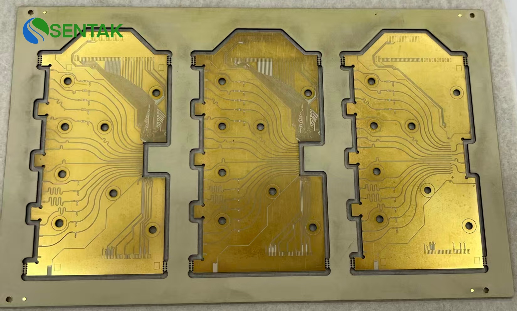
Additional considerations include copper foil roughness (ultra-low roughness HVLP copper reduces skin-effect loss in high-frequency applications) and thermal expansion coefficient (CTE) matching to prevent solder joint fatigue in temperature-cycling environments. When scaling from prototype to production, partnering with a manufacturer that specializes in high-frequency PCB and PCBA manufacturing—such as SENTAK, which offers custom RF/microwave PCB solutions with precise material selection and tight tolerance control—ensures that substrate properties are consistently maintained across production runs, avoiding performance variability.
2. Impedance Control: Non-Negotiable for Signal Integrity
Impedance mismatch is the leading cause of signal reflection, reduced transmission efficiency, and poor system performance in RF and microwave circuits. The goal is to maintain a consistent characteristic impedance (Z₀) across all transmission lines, with 50 Ω being the industry standard for most RF applications (75 Ω for video/RF broadcast systems). Impedance control is determined by three key factors: substrate thickness (h), trace width (W), and dielectric constant (Dk) of the substrate, as defined by microstrip and stripline design formulas.
To achieve precise impedance control (typically ±5% for RF, ±3% for microwave/millimeter-wave), follow these steps: (1) Use impedance calculation tools or electromagnetic simulation software (e.g., ADS, HFSS) to determine the required trace width for the chosen substrate; (2) Maintain uniform trace width throughout the transmission line—avoid sudden widening or narrowing, which causes impedance discontinuities; (3) Ensure the reference ground plane directly below the transmission line is complete and unbroken, as gaps or slots in the ground plane disrupt impedance and increase signal radiation. For critical applications, SENTAK’s engineering team provides pre-production impedance simulation and DRC (Design Rule Check) services to validate trace designs, ensuring compliance with target impedance specifications before manufacturing.
3. Layout and Routing: Minimizing Parasitics and Interference
RF and microwave PCB layout is governed by the principle of minimizing parasitic inductance, capacitance, and EMI, as these effects become dominant at high frequencies. Key layout guidelines include:
- Short, Straight, and Direct Routing: Keep transmission lines as short as possible to reduce insertion loss and phase shift. Avoid unnecessary bends; if bends are required, use 45° angles or rounded corners (radius ≥ 0.5 mm) instead of 90° angles, which cause impedance change suddenly and signal reflection. Never use serpentine routing for RF signals, as it increases trace length and parasitic inductance.
- Physical Partitioning: Separate RF/microwave circuits from digital and power circuits to minimize EMI coupling. Use dedicated ground planes for each circuit type, and ensure RF components (e.g., amplifiers, filters, antennas) are isolated from noise sources (e.g., microcontrollers, switching regulators). For multi-layer PCBs, place RF transmission lines on outer layers with a solid ground plane directly below, and route digital signals on inner layers.
- Minimize Via Usage: Each via introduces parasitic inductance (≈0.1–0.3 nH) and capacitance, which degrades impedance continuity. Avoid vias on critical transmission lines; if a via is necessary (for layer transitions), place multiple ground vias adjacent to the signal via (spaced ≤ λ/10) to create a low-impedance ground path and suppress parasitic effects.
- Component Placement: Place RF components (e.g., matching networks, oscillators) close to each other to minimize trace length. Keep matching network components (inductors, capacitors) as close to the device pins as possible to reduce parasitic effects, and use high-frequency components (e.g., NP0 capacitors, air-core inductors) with low parasitic parameters.
4. Grounding and Shielding: Mitigating EMI and Ensuring Stability
Proper grounding is critical for RF and microwave PCBs, as it provides a low-impedance return path for signals, reduces EMI, and stabilizes circuit performance. Use a solid, unbroken ground plane for RF circuits—avoid splitting the ground plane, as this creates high-impedance return paths and causes signal reflection. For multi-layer PCBs, a dedicated ground layer directly below the RF signal layer is mandatory.
Ground vias play a key role in grounding: place them densely around RF components (e.g., transistor pins, shielded enclosures) and along transmission lines to ensure a continuous ground connection across layers. The spacing between ground vias should not exceed λ/20 (where λ is the wavelength of the highest operating frequency) to prevent resonant effects. Additionally, use shielding enclosures (e.g., metal cans) for sensitive RF modules (e.g., low-noise amplifiers, oscillators) to block external EMI and prevent internal signals from radiating to other parts of the PCB.
5. Thermal Management: Protecting High-Power RF Components
High-power RF components (e.g., power amplifiers, microwave transistors) generate significant heat, which can degrade performance, reduce component lifespan, and cause thermal drift in impedance. To address this, integrate thermal management features into the PCB design: (1) Use high-thermal-conductivity substrates (e.g., aluminum-based PCBs, Rogers RT/duroid 6035HTC) for high-power applications; (2) Add thermal vias beneath high-power components to conduct heat to the ground plane or a heatsink; (3) Use large copper pads for heat dissipation, and ensure adequate spacing between heat-generating components to avoid thermal crosstalk.
6. Design Validation and Manufacturing Considerations
Before production, validate the RF/microwave PCB design using electromagnetic simulation software (ADS, HFSS, or CST) to optimize impedance, minimize signal loss, and predict EMI performance. Simulate key parameters such as S-parameters (S11 for return loss, S21 for insertion loss), VSWR (Voltage Standing Wave Ratio), and phase shift to ensure compliance with design specifications. For prototype validation, use a Vector Network Analyzer (VNA) to measure these parameters and refine the design if necessary.
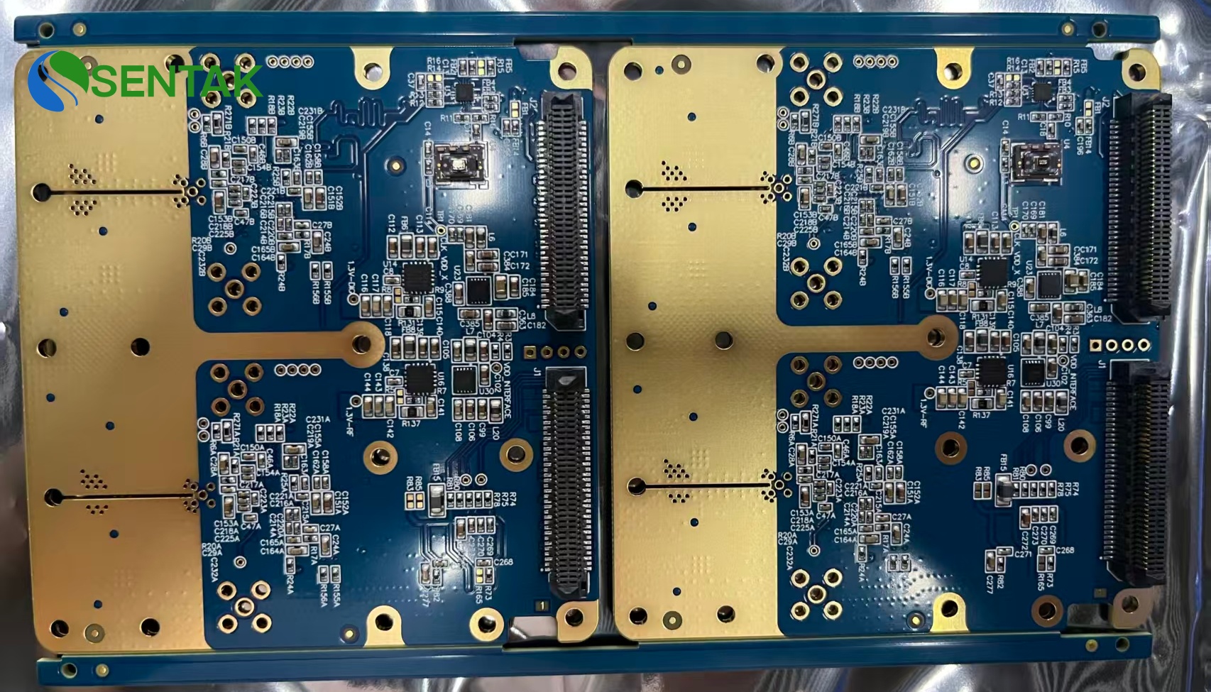
Manufacturing tolerances also impact RF performance: ensure the manufacturer can maintain tight control over substrate thickness (±5%), trace width (±0.03 mm), and copper thickness to preserve impedance accuracy. SENTAK, with its expertise in high-precision PCB and PCBA manufacturing, offers prototype to mass production services for RF and microwave applications, including impedance-controlled PCBs, multi-layer boards up to 30 layers, and custom surface finishes (e.g., ENIG,沉银) to ensure long-term reliability in harsh environments. Their 100% testing policy (flying probe or e-test) and flexible lead times further support efficient design iteration and production scalability.
Conclusion
RF and microwave PCB design requires a holistic approach that integrates material science, impedance control, layout optimization, and manufacturing expertise. By following these guidelines—prioritizing substrate selection, precise impedance control, careful layout and routing, robust grounding, thermal management, and rigorous validation—engineers can develop high-performance, reliable RF systems that meet the demands of modern applications (5G, automotive radar, IoT, satellite communication). Partnering with a specialized manufacturer like SENTAK ensures that design intent is translated into consistent, high-quality PCBs and PCBAs, reducing time-to-market and minimizing performance risks.