In the world of electronics, the demand for compact, efficient, and powerful devices has led to the rise of multilayer pcb fabrication. This technology is critical for modern circuit boards, allowing them to integrate multiple layers of circuitry in a single unit. The significance of multilayer PCB fabrication extends beyond mere convenience; it addresses common pain points in the design and manufacturing processes of electronic devices. As electronic devices become increasingly intricate, the need for multilayer PCBs becomes essential to meet both performance and space requirements.
What is Multilayer PCB Fabrication and How It Works
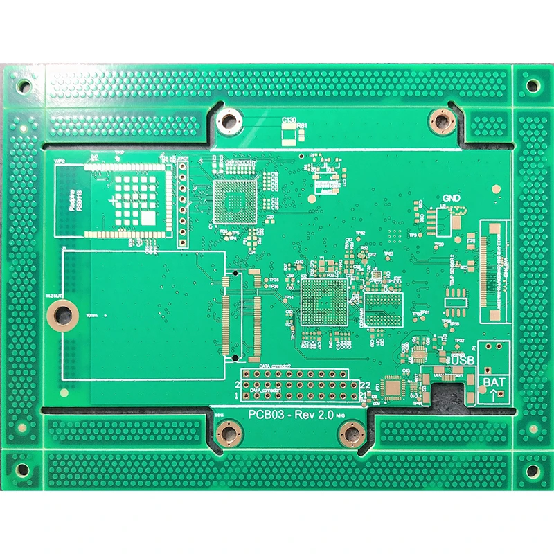
Multilayer PCB fabrication refers to the process of constructing printed circuit boards with three or more layers of conductive pathways. These layers are stacked and interconnected through vias, which are small plated holes that allow electrical connections between layers. According to a recent report by the industry authority IPC International, multilayer PCBs reduce space by about 60%, making them an ideal choice for devices where real estate is limited.
The fabrication process starts with the selection of materials, usually a combination of conductive copper layers and insulating materials. The base materials undergo a series of processes, including etching, layering, and lamination, to create a final product that is reliable and effective. Notably, advances in technology have improved the accuracy of multilayer PCB fabrication, resulting in a defect rate reduction of approximately 15% compared to traditional methods.
Application Scenarios
Multilayer PCBs find application across numerous fields, including:
- Consumer Electronics: Smartphones and laptops often utilize multilayer PCBs to fit complex circuits into compact form factors.
- Automotive Industry: Modern vehicles employ multilayer PCB technology for advanced systems such as infotainment controls and safety features.
- Telecommunications: High-speed data transfer applications leverage multilayer PCBs to accommodate dense circuitry without signal loss.
- Medical Devices: Critical medical equipment utilizes multilayer PCBs for compact, reliable, and efficient performance.
The versatility of multilayer PCBs in these fields highlights their importance in driving technological advancement.
Brief Description of Advantages
The advantages of multilayer PCB fabrication are substantial, making them a cornerstone of modern electronics:
- Space Efficiency: By combining multiple layers, multilayer PCBs can house extensive circuitry in a smaller footprint, which is crucial for portable devices.
- Enhanced Performance: With better heat dissipation and improved electrical performance, multilayer PCBs can support high-frequency applications with minimal interference.
- Cost-effectiveness: Although the initial fabrication cost may be higher, multilayer PCBs can significantly lower overall production costs by reducing the number of components needed.
- Improved Reliability: The construction technique used in multilayer PCBs enhances durability, allowing them to withstand the rigors of demanding applications.
Picture Location
Next Steps for Users
If you are interested in exploring multilayer PCB solutions further, we recommend visiting SENTAK's online user guide. It provides detailed instructions on selecting the right materials, understanding design specifications, and optimizing your PCB for performance. This resource is invaluable for engineers and hobbyists alike as you navigate your project requirements.
FAQ
Q: What is the typical number of layers in a multilayer PCB?
A: Multilayer PCBs can range anywhere from 4 to over 20 layers, depending on the complexity of the design and electrical requirements.
Q: How does multilayer PCB fabrication differ from standard PCBs?
A: Standard PCBs usually consist of one or two layers, while multilayer PCBs incorporate multiple layers that enable complex circuits to fit into a compact design.
Q: What materials are commonly used in multilayer PCBs?
A: Typical materials include copper for conductive pathways and FR-4 (glass-reinforced epoxy laminate) for insulation and structural integrity.
Conclusion
Multilayer PCB fabrication is an advanced technology that addresses essential user needs in various applications, offering both versatility and reliability. If you are gearing up for your next electronic project, consider leveraging the capabilities of multilayer PCBs. For further understanding or to initiate a trial, please check out SENTAK's series of products and user recommendations.