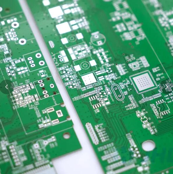
Multilayer PCBs represent an advanced evolution of standard printed circuit boards. Unlike single or double-layer PCBs, multilayer PCBs consist of three or more layers of electronic components and conductive traces separated by insulating materials. This multilayer structure allows for higher component density, more complex designs, and a reduction in board size and weight.
These advantages make multilayer PCBs ideal for compact and portable electronic devices, such as smartphones, laptops, and advanced medical equipment.
The Multilayer PCB Manufacturing Process
The process of manufacturing multilayer PCBs is complex and requires high precision to ensure the functionality and reliability of the final product. The following steps outline the full process:
1. Design and Layout
The first step in multilayer PCB production is the design and layout, which translates conceptual functionality into a practical blueprint. Key activities include:
- Requirement analysis and schematic design
- Component selection
- Determining the number of layers and their sequence
- Component placement and routing
- Signal integrity analysis
- Heat dissipation planning
- Design for manufacturability (DFM) checks
- Final design review
2. Material Selection
Selecting high-quality materials is critical for multilayer PCBs, as it affects thermal, electrical, and mechanical performance. Commonly, FR4 (glass-reinforced epoxy laminate) is used. Considerations during material selection include:
- Research and compatibility analysis
- Quality standards compliance
- Performance evaluation
- Cost assessment
3. Layer Preparation
This step forms the structural foundation of the PCB and organizes conductive pathways. Activities include:
- Prepreg preparation (resin-impregnated layers)
- Copper foil processing and organization
- Assigning functions for each layer (signal, ground, power plane)
4. Circuit Pattern Printing
Precise circuit pattern creation is achieved using photosensitive films and UV exposure. The process involves:
- Coating inner layer cores with photosensitive film
- UV printing of the circuit pattern
- Etching unexposed areas to form the desired copper traces
5. Layer Alignment and Lamination
Accurate alignment and bonding of layers is essential for PCB performance:
- Layer alignment using registration holes or pins
- Lamination under heat and pressure to bond layers together
- Melting prepreg to ensure cohesion between layers
6. Drilling
Drilling provides vias for electrical connections between layers and holes for through-hole components. Techniques include:
- CNC drilling machines for precision
- Micro-drills for intricate patterns
- Laser drilling for advanced applications
7. Plating and Copper Deposition
Copper plating ensures conductivity and reliable signal transmission:
- Electroplating the board and via walls
- Ensuring proper electrical connections between layers
8. Outer Layer Imaging and Development
Outer layers are prepared using photosensitive film and exposure equipment:
- Coating the outer layers with photosensitive film
- Exposing and developing patterns for etching
9. Etching and Layer Definition
Etching removes unwanted copper to define the final circuit patterns:
- Using chemical solutions and protective resists
- Ensuring precise circuit formation on outer layers
10. Solder Mask Application
The solder mask protects copper surfaces from oxidation and prevents solder bridges between pads. Steps include:
- Applying solder mask across the PCB surface
- Leaving pads exposed for component soldering
- Ensuring protection and electrical integrity
11. Surface Finish
Surface finishes protect pads and enable reliable soldering:
- Common finishes include HASL and OSP
- Provides oxidation protection and solderable surfaces
12. Silkscreen Printing
Component labels and markings are printed for assembly guidance and troubleshooting.
13. Electrical Testing
Multilayer PCBs undergo rigorous electrical testing to confirm that design requirements are met and to identify any defects.
14. Cutting and Profiling
The PCB panels are cut into their final shapes and sizes, ready for inspection and assembly.
15. Final Inspection and Quality Control
A thorough inspection ensures that each PCB meets quality standards and is free from physical or functional defects.
Conclusion
Multilayer PCB manufacturing is a highly systematic process, including design, material selection, layer preparation, circuit printing, lamination, drilling, plating, outer layer imaging, etching, solder mask application, surface finishing, and final inspection. Each step is critical for producing reliable, high-performance multilayer PCBs.
FAQ
Q1: What factors influence the cost of multilayer PCB fabrication?
Key factors include the number of layers, board size, materials, circuit complexity, and manufacturing technology.
Q2: Which industries commonly use multilayer PCBs?
Multilayer PCBs are widely used in telecommunications, automotive, medical devices, consumer electronics, and aerospace industries.
Q3: What advantages do multilayer PCBs offer over single or double-layer boards?
They provide higher circuit density, smaller size, better signal integrity, improved power distribution, and enhanced EMI performance.
Q4: What is the typical layer count for multilayer PCBs?
Most multilayer PCBs have 4 to 16 layers, although more layers are possible depending on design complexity.
Q5: How does automation impact multilayer PCB manufacturing?
Automation enhances precision, reduces errors, and speeds up production in drilling, imaging, and solder mask application pro
Don’t wait—our team provides high-quality multilayer PCB manufacturing and assembly with fast turnaround and global shipping. Upload your Gerber files or request a consultation today!