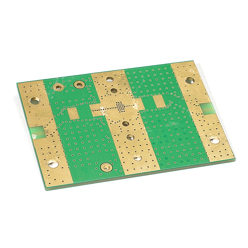
In today's fast-paced world, seamless communication is crucial for businesses to thrive. If you've been facing issues with slow data transmission, signal degradation, or interference in your communication systems, I’m here to help you navigate the complexities surrounding high-frequency printed circuit boards (PCBs). By following these clear and actionable steps, you can significantly enhance your communication capabilities utilizing high-frequency pcbs from SENTAK.
The focus on high-frequency PCBs represents a transformative approach to improving communication systems, which is essential for reliability and efficiency. These advanced PCBs enable faster signal propagation, reduced latency, and improved signal integrity crucial for applications ranging from telecommunications to IoT devices. Let’s delve into each step to adopt high-frequency PCBs effectively and tackle your communication challenges head-on.
Understanding High-Frequency PCBs
High-frequency PCBs are designed to operate reliably at frequencies exceeding 1 GHz. The intricacies of such boards encompass precise materials and manufacturing techniques, like:
- Low-loss materials: These reduce signal loss and improve overall performance.
- Controlled impedance: Ensures signal integrity through consistent electrical characteristics.
- Minimized crosstalk: Filters out unwanted interference between signal traces.
Integrating these features helps your systems support a broader range of applications efficiently. Businesses that adopt high-frequency PCBs often report up to a 30% increase in operational speed.
Step-by-Step Implementation for Improvement
-
Assess Your Current System: Identify the specific communication issues you face, such as weak signals or inefficiencies in data transfer. Understanding your current setup is crucial.
-
Select the Right High-Frequency PCB: Work with SENTAK to choose a PCB that meets your technical specifications. Look for features like:
- Frequency ratings (1 GHz and above)
- Material used (Teflon, Rogers, etc.)
- Layer count and thickness
-
Prototype Development: Use SENTAK’s expertise to develop prototypes for testing. This allows you to evaluate performance under real-world conditions. We emphasize 100% inspection at this stage to ensure all parameters meet your standards.
-
Testing and Validation: Conduct rigorous testing using industry standards such as ASTM and DIN to measure performance metrics. Metrics should include:
- Signal integrity
- Thermal management
- Electrical performance
-
Full-Scale Deployment: Upon successful validation, proceed with full deployment across communication systems. This phase enhances scalability and efficiency.
-
Ongoing Evaluation: Regularly assess performance. Gather data on operational efficiency and make adjustments as necessary.
Addressing Common Challenges
While transition to high-frequency PCBs can revolutionize your communication systems, it’s not without its challenges. Some potential hurdles include:
- Technical Expertise: You may lack in-house expertise to troubleshoot complex issues. Partner with SENTAK for training and support.
- Integration Issues: High-frequency PCBs may not be compatible with legacy systems. Ensure that all components are evaluated for compatibility.
Overcoming Challenges
- Training Programs: Consider workshops hosted by SENTAK to adequately prepare your team for the technical demands of high-frequency PCBs.
- Thorough Testing: Implement a phased testing approach to identify problems early on before full-scale deployment.
Tools and Resources for Enhanced Efficiency
To maximize your outcomes with high-frequency PCBs, consider utilizing:
- Simulation Software: Programs like HFSS or ADS can help visualize potential signal issues before physical production.
- Design Tools: Collaborative tools that allow remote adjustments and reviews streamline communication between your design team and manufacturers.
Quick Recap to Motivate Action
To summarize, the journey towards enhancing your communication systems with high-frequency PCBs involves:
- Assessing your current communication challenges.
- Collaborating with SENTAK to find the right PCB solution.
- Prototyping, testing, and validating to ensure optimal performance.
- Deploying and consistently evaluating the systems for continual improvement.
By implementing these steps, your business can expect not only improved communication efficiency but also a potential increase in productivity. Don't wait! Start enhancing your communication solutions with high-frequency PCBs from SENTAK today.
For more information and resources, visit SENTAK. With our aid, you can resolve issues quickly and effectively, leading to robust communication systems that stand the test of time. Let’s get started!