High-frequency printed circuit boards (PCBs) are designed for applications requiring fast signal transmission and low-loss characteristics. These advanced PCBs serve industries like telecommunications, aerospace, and automotive, addressing challenges with signal integrity and electromagnetic interference. Whether you are an engineer looking for optimal performance or a business seeking to improve product reliability, this guide on high-frequency pcbs will help solve your design issues by providing a comprehensive understanding of their properties and manufacturing processes.
Understanding High-Frequency PCBs: Terminology, Principles, and Background
High-frequency PCBs, often used in radio frequency (RF) applications, operate at frequencies above 1 GHz. This section covers some key terminology and principles that help decipher the complex world of these boards:
- Dielectric Constant (Dk): A measure of a material's ability to store electrical energy. High-frequency applications usually require dielectric materials with a Dk of less than 3.0.
- Loss Tangent (Df): Indicates the inherent loss of signal strength in a PCB material. Materials with a Df lower than 0.02 are preferred for high-frequency operations to ensure minimal signal degradation.
- Microstrip and Stripline: These are configurations used in PCB design that determine how the traces are routed on the board. Microstrip has a ground plane underneath the trace, while a stripline is sandwiched between two ground planes, providing better shielding.
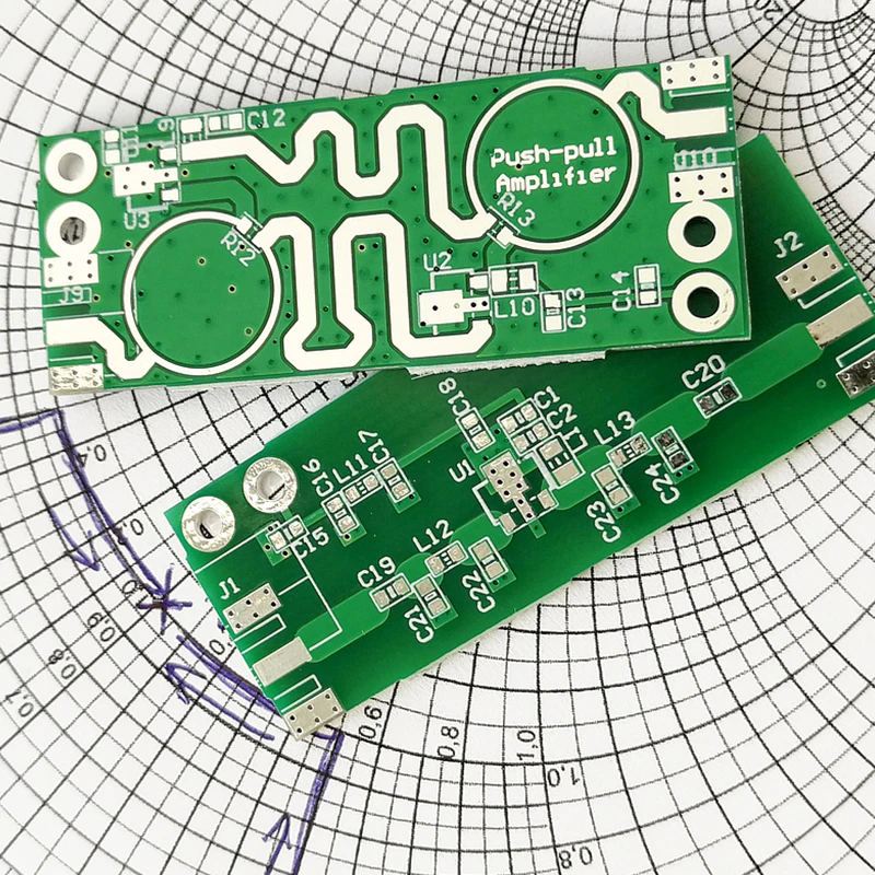
In-Depth Guide to High-Frequency PCB Design and Manufacturing
Creating an efficient high-frequency PCB involves several steps, each with specific tools and examples for successful execution.
Step 1: Material Selection
Choose the right substrate material. Options like Rogers, Teflon, and FR-4 are standard. For high-frequency PCBs, materials such as Rogers 5880 (Dk 2.2, Df 0.0009) provide excellent performance under 10 GHz.
Step 2: Design Simulation
Utilize simulation software such as ANSYS HFSS or Keysight ADS to model the PCB. This allows you to visualize signal integrity, electromagnetic interference, and performance before fabrication.
Step 3: Trace Geometry
Define trace widths and spacing based on frequency and Dk values. For example, a 10 GHz signal may require a trace width of about 0.25 mm and a space of 0.25 mm to achieve a characteristic impedance of 50 ohms.
Step 4: Layer Stack-up Configuration
Design the appropriate stack-up, typically involving multiple layers for RF applications. A common configuration is a 2-layer PCB with a microstrip on the outer layer and a ground plane on the inner layer.
Step 5: Manufacturing Process
Work with a reputable manufacturer like SENTAK to produce your design. Ensure they use advanced techniques such as laser drilling for precision and accuracy, which has been shown to reduce manufacturing defects to under 0.5%.
Step 6: Testing and Validation
After manufacturing, perform testing using a vector network analyzer (VNA) to measure reflection and insertion loss. Products that show less than 0.5 dB of insertion loss at 10 GHz are considered highly efficient.
FAQ on High-Frequency PCBs
- What types of applications use high-frequency PCBs? High-frequency PCBs are commonly used in telecommunications, radar systems, and medical devices.
- How do I determine the right material for my PCB? Consider the operating frequency, dielectric constant, and loss tangent when selecting your material.
- What testing methods should I employ? Utilize methods like TDR (Time Domain Reflectometry) and VNA to ensure signal integrity and measure losses accurately.
Advanced Skills and Extended Reading
For engineers looking to delve deeper into high-frequency PCB design, literature such as "RF Circuit Design" by Chris Bowick provides advanced methodologies for RF PCB layout and design techniques. Furthermore, resources from the IEEE Xplore Digital Library offer extensive research papers on advancements in high-frequency technology.
Conclusion: Recommended Products/Services
For superior high-frequency PCB solutions, contact SENTAK. Their commitment to quality and advanced technology ensures that your designs reach optimal performance levels. You can browse their offerings at SENTAK PCB.