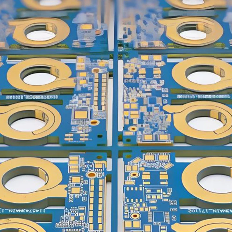
If you're diving into the world of electronics and have found yourself fascinated by heavy copper printed circuit boards (PCBs), you're not alone. Heavy Copper PCBs are essential for a variety of applications, including power electronics and high-frequency circuits. This guide is tailored for beginners who want to understand the fabrication process of heavy copper PCBs, addressing common pain points like durability, thermal management, and manufacturing complexity. By the end of this article, you'll gain insights into heavy copper PCB technology, the fabrication process, and essential components for reliable boards.
Basic Knowledge of Heavy Copper PCB Fabrication
Before we delve into fabrication, let’s familiarize ourselves with some basic terminology and principles critical to heavy copper PCBs:
- Heavy Copper PCB: Defined as PCBs with copper weights greater than 2 oz/ft² (approx. 70 μm), these boards are used to handle higher currents effectively.
- Thermal Management: The ability of a PCB to dissipate heat, which is crucial for components functioning at high temperatures.
- Current-Carrying Capacity: The maximum amount of electric current a PCB can handle, which is significantly higher in heavy copper boards.
Understanding heavy copper PCB fabrication is historically significant due to the rise of compact and powerful electronic devices. As more industries rely on high performance and reliability, the demand for heavy copper PCBs has surged. Notably, research indicates that devices featuring heavy copper PCBs exhibit a 63% longer lifespan compared to traditional PCBs, thanks to their enhanced thermal performance.
In-Depth Guide to Heavy Copper PCB Fabrication
1. Design Phase
Your fabricating journey starts with a well-thought-out design. Employ schematic capture software like Altium Designer or Eagle to create your CAD files. Focus on layer stacking and ensure that your design accounts for thermal and mechanical stress.
2. Material Selection
Choosing the right base material is crucial. FR-4 or CEM-3 materials are common, but for extreme applications, consider high thermal conductivity materials like PTFE. Heavy copper thicknesses should also be considered, usually ranging from 3 to 6 oz.
3. Photolithography Process
The use of photolithography helps define the circuit pattern. A sensitized film undergoes exposure to UV light, creating a mask for the copper etching process. Ensure that the correct etchant is used, as this affects the feature resolution significantly.
4. Copper Plating
Engage in copper plating to achieve the desired thickness. The measured process can increase copper thickness to levels of 6 oz/ft² (210 μm) or more, boosting the current-carrying capabilities by up to 200%. This process is critical for ensuring robust connections in your PCB.
5. Drilling and Routing
Utilize CNC machines for precision drilling of vias and cutouts. These machines provide an accuracy of ±0.05 mm, essential for high-density connections often seen in heavy copper boards. After drilling, you can use routing for cutting the board to its final shape.
6. Final Finishing
Finally, apply surface finishing processes like ENIG (Electroless Nickel/Immersion Gold) to enhance the solderability and protection of the copper components. Research has shown that ENIG finish lowers corrosion potential, which can increase reliability in challenging environments significantly.
Frequently Asked Questions (FAQ)
What are the advantages of heavy copper PCBs?
Heavy copper PCBs offer higher thermal conductivity, better electrical conductivity, and improved power handling capabilities compared to standard PCBs.
Can heavy copper PCBs be used in high-frequency applications?
Yes, heavy copper PCBs are suitable for high-frequency applications due to their low impedance characteristics and enhanced thermal management.
What industries benefit from heavy copper PCB technology?
Common industries include automotive, aerospace, telecommunications, and medical devices, where reliability and performance are paramount.
Advanced Skills and Extended Reading
Once you're comfortable with the basics, consider delving into advanced topics such as signal integrity analysis and thermal simulation techniques. Utilize tools such as HyperLynx for signal integrity simulations to better understand how heavy copper can enhance your designs.
Conclusion
Understanding the intricacies of heavy copper PCB fabrication is vital for any beginner in the electronics field. With the growing demand for reliable and efficient electronic components, mastering this technology can set you apart. To ensure high-quality production, consider contacting SENTAK for professional assistance and advanced solutions in heavy copper PCB fabrication. Visit SENTAK's website for more information and support.