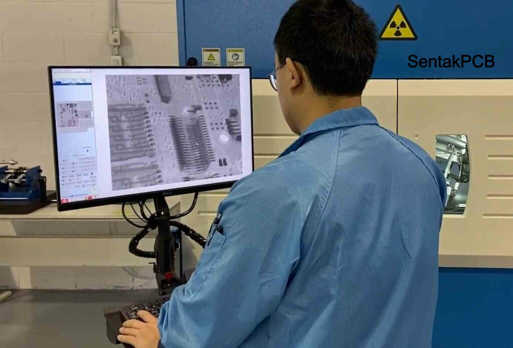
In the world of electronics manufacturing, the Printed Circuit Board Assembly (PCBA) process is the heartbeat of modern innovation. From smartphones to medical devices, the reliability of these intricate boards determines the success of the final product. As electronic devices continue to shrink in size while growing in complexity, ensuring the integrity of solder joints and hidden interconnections has become a monumental challenge. This is where X-ray inspection technology steps in — not just as a quality control tool, but as a necessity.
What X-ray Inspection Reveals
X-ray technology in PCB assembly is not merely about looking for obvious defects; it is about process verification and reliability assurance. Here are the key defects that X-ray inspection captures with precision:
- Solder Voiding: Voids are pockets of trapped gas within a solder ball. While small voids are sometimes acceptable, excessive voiding can lead to thermal hotspots and mechanical failure. X-ray provides precise measurement of void ratios to ensure they fall within industry standards like IPC-A-610.
- Bridging: In fine-pitch components, even a microscopic excess of solder can create a short circuit. X-ray reveals these bridges clearly, especially in areas where they are hidden under the component.
- Head-in-Pillow (HiP): One of the most insidious defects in BGA assembly, HiP occurs when the solder ball melts but fails to merge with the paste. The connection looks physically connected but is electrically open. Only advanced 2D or 3D X-ray systems can detect the subtle gap indicative of this defect.
- Alignment: X-ray confirms that components are placed correctly, ensuring that ball-to-pad registration is accurate.
The Shift from 2D to 3D CT Scanning
For years, 2D X-ray machines provided a top-down shadow image. While useful, this technology has limitations — specifically, the superposition of images. Because the image is a composite of all layers, a defect on the top layer might be obscured by a component on the bottom.
Today, the gold standard for high-reliability manufacturing is 3D Computed Tomography (CT), particularly AXI (Automated X-ray Inspection) . By rotating the board and capturing multiple angles, these systems create cross-sectional slices of the board. This allows manufacturers to isolate specific layers, measure void volumes with mathematical accuracy, and inspect double-sided assemblies without overlapping interference.
Cost Avoidance vs. Cost of Test
Some manufacturers hesitate to invest in advanced X-ray inspection, viewing it as an expensive bottleneck. However, in the context of total manufacturing cost, X-ray inspection is a powerful tool for cost avoidance.
Consider the alternative: a defect escaping to the field. For a medical device or automotive control unit, the cost of a single field failure — including recalls, legal liability, and brand damage — far exceeds the cost of implementing robust inspection. Furthermore, by using X-ray inspection for process control rather than just final audit, manufacturers can detect trends early. If voiding rates begin to increase, engineers can adjust the reflow profile or solder paste volume immediately, preventing the mass production of defective units.
Integrating X-ray into Smart Manufacturing
In the era of Industry 4.0, X-ray inspection is no longer an isolated station. Modern X-ray systems are integrated into the manufacturing execution system (MES). They provide real-time data feedback to solder paste printers and reflow ovens. This closed-loop process control ensures that quality is built into the product, not just inspected at the end.
For companies that prioritize high-mix, high-reliability production, investing in advanced X-ray capabilities is non-negotiable. It demonstrates a commitment to quality that builds trust with clients in sectors like aerospace, automotive, and industrial controls.
Our Commitment at SENTAK
At SENTAK, we understand that inspection is not just about finding defects — it is about engineering confidence. As a specialized PCB and PCBA manufacturer, we recognize that the reliability of a final product is determined by the processes hidden beneath the surface. We integrate advanced X-ray inspection technologies into our production workflow, ensuring that every BGA, QFN, and hidden interconnection meets the highest standards of integrity. For us, quality assurance is not an afterthought; it is embedded into every stage of assembly, from solder paste application to final verification. This commitment allows us to deliver assemblies that perform reliably in the most demanding applications.
Conclusion
As electronics continue to trend toward miniaturization and higher density, the “blind spots” of traditional inspection methods become critical vulnerabilities. X-ray inspection technology provides the transparency needed to ensure that what lies beneath the surface is flawless. It transforms the assembly process from a reactive “test and reject” model into a proactive “predict and control” discipline.
For any manufacturer serious about quality — whether in consumer electronics or life-critical medical devices — X-ray inspection is not just important; it is indispensable. It is the lens through which we ensure the invisible does not become the unreliable.