The Core SMT Assembly Procedure: A Symphony of Precision
A successful SMT line is a marvel of engineering coordination, where each stage must be flawlessly executed. Here’s a breakdown of the key steps:
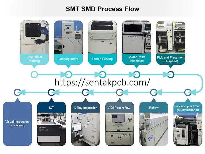
Solder Paste Printing: The process begins with a stencil, a laser-cut stainless-steel sheet, aligned perfectly over the PCB. Solder paste — a sticky mixture of tiny solder balls and flux — is spread across the stencil, depositing precise amounts onto the component pads. This step is crucial; too little paste causes a weak joint, too much can cause shorts.
Component Placement: This is where high-speed automation truly shines. Advanced pick-and-place machines, guided by sophisticated vision systems, collect components from reels, trays, or sticks. They then position them at incredible speeds and with micron-level accuracy onto the solder paste deposits. Modern machines can place tens of thousands of components per hour, handling parts smaller than a grain of sand.
Reflow Soldering: The populated PCB then travels through a reflow oven on a conveyor belt. This oven subjects the board to a carefully profiled temperature curve. The paste first melts (reflows), wetting the component leads and PCB pads to form a permanent metallurgical bond, then cools to create solid, reliable electrical connections. This profile is critical to prevent defects like tombstoning or bridging.
Inspection and Testing: Quality is non-negotiable. Automated Optical Inspection (AOI) systems use cameras to check for placement accuracy, solder joint quality, and missing components. For complex boards with hidden connections, X-ray inspection is used to examine solder joints under components like BGAs. Finally, electrical tests verify the board’s functionality.
The Future is Now: Key Trends Shaping SMT Assembly
The drive for smaller, faster, and more connected devices continues to push SMT technology forward. Here are the dominant trends:
The March of Miniaturization: Components like 01005 (0.4mm x 0.2mm) and even smaller are becoming commonplace. This demands unprecedented precision in stencil printing, placement, and inspection, pushing machinery and material science to new limits.
Embracing Industry 4.0 and AI: The smart factory has arrived. Modern SMT lines are integrated with IoT sensors, collecting real-time data on machine performance, process parameters, and product quality. Artificial Intelligence (AI) algorithms analyze this data to predict maintenance needs, optimize the reflow profile dynamically, and automatically flag potential defects, transitioning from detection to prevention.
Advanced Packaging Integration: Technologies like System-in-Package (SiP) and embedded components blur the lines between PCB and package. SMT lines are adapting to handle these heterogeneous integration challenges, placing entire functional modules alongside traditional components.
The Green Imperative: Sustainability is moving from a nice-to-have to a must-have. This drives the adoption of lead-free and halogen-free solders, low-VOC (volatile organic compound) cleaning chemistries, and energy-efficient machinery, aligning manufacturing with global environmental goals.
Navigating the Future with a Trusted Partner
Staying ahead of these trends requires more than just advanced machinery; it demands deep expertise, continuous process optimization, and a commitment to quality at every step. This is where the choice of manufacturing partner becomes critical.
At SENTAK PCB, we live at the intersection of precision and innovation. Our state-of-the-art SMT production lines are equipped with the latest high-speed placement systems, advanced SPI/AOI, and fully monitored reflow ovens, capable of handling the most demanding designs — from ultra-dense consumer electronics to reliable automotive and industrial controllers.
More than just a PCB and PCBA factory, we function as an extension of your engineering team. We understand that robust manufacturing is built on a foundation of exceptional PCB fabrication. By controlling the entire process from PCB base material to finished assembled board, we ensure seamless compatibility, stringent quality control, and faster time-to-market for your products.
The evolution of SMT is a story of relentless pursuit of precision, intelligence, and responsibility. As devices continue to shrink and smarten, the processes that build them will only grow more sophisticated.
What’s the most challenging aspect of miniaturization you’ve faced in your designs? Share your thoughts in the comments below.
SENTAK PCB empowers innovation by delivering high-quality, reliable PCB fabrication and PCBA assembly services. Leveraging advanced SMT technology and a commitment to excellence, we help engineers and businesses turn complex concepts into reality. Ready to build the future? Let’s connect.